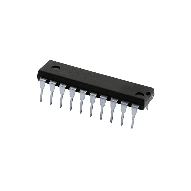
74373 IC Octal Transparent Latch with 3-State
The IC 74373 contains eight D-type transparent latches. It captures data from inputs D0–D7 while the latch enable (LE) signal remains HIGH. When LE goes LOW, the chip holds the last data on its inputs.
Each output (Q0–Q7) connects to a three-state buffer controlled by an output enable (OE¯) pin. When you drive OE¯ LOW, the device drives the latched data onto the outputs. When you drive OE¯ HIGH, the outputs enter a high-impedance state and disconnect from the bus.
Designers use the 74373 to latch data temporarily, buffer buses, and manage bidirectional data flow in high-speed digital systems.
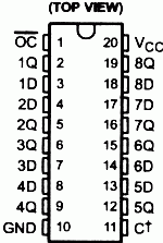
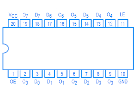
Pin Configuration (DIP-20)
| Pin | Name | Description |
|---|---|---|
| 1 | OE¯ | Output Enable (LOW = active) |
| 2 | Q0 | Output Bit 0 |
| 3 | D0 | Input Bit 0 |
| 4 | D1 | Input Bit 1 |
| 5 | Q1 | Output Bit 1 |
| 6 | Q2 | Output Bit 2 |
| 7 | D2 | Input Bit 2 |
| 8 | D3 | Input Bit 3 |
| 9 | Q3 | Output Bit 3 |
| 10 | GND | Ground |
| 11 | Q4 | Output Bit 4 |
| 12 | D4 | Input Bit 4 |
| 13 | D5 | Input Bit 5 |
| 14 | Q5 | Output Bit 5 |
| 15 | Q6 | Output Bit 6 |
| 16 | D6 | Input Bit 6 |
| 17 | D7 | Input Bit 7 |
| 18 | Q7 | Output Bit 7 |
| 19 | LE | Latch Enable |
| 20 | VCC | +5V Supply |
Key Features
Stores 8 bits and outputs them when enabled
Provides three-state outputs for bus control
Supports transparent latching and edge storage
Works with TTL logic levels
Drives external loads directly
Available in DIP-20 and SOIC-20
Applications
Latch address or data lines in microprocessor systems.
Drive shared buses without conflicts.
Hold temporary output values in I/O devices.
Implement memory address registers.
Expand microcontroller port capacity.
Store display data for panels.
Use in digital signal pipelines.
Buffer long PCB traces to reduce loading.
Build parallel-to-serial interfaces.
Teach transparent latch operation in labs.
Specifications Table
| Parameter | Value |
|---|---|
| Logic Family | TTL |
| Function | Octal Transparent Latch |
| Bits Stored | 8 |
| Inputs | D0–D7, LE, OE¯ |
| Outputs | Q0–Q7 |
| Input HIGH Voltage | ≥ 2.0V |
| Input LOW Voltage | ≤ 0.8V |
| Output HIGH Voltage | ≥ 2.4V ‘ |
| Output LOW Voltage | ≤ 0.4V |
| Propagation Delay | ~15 ns |
| Max Frequency | ~35 MHz |
| Supply Voltage | 4.75–5.25V |
| Operating Temp | 0–70°C |
| Package Type | DIP-20 |