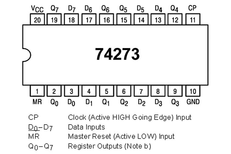
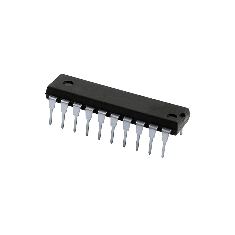

74273 IC Octal D-Type Flip-Flop with Clear
The IC 74273 contains eight edge-triggered D-type flip-flops. It captures data from inputs D0–D7 on the rising edge of the clock (CP) and drives outputs Q0–Q7 directly. The clear (CLR) input forces all outputs to LOW when you drive it LOW.
The chip drives high-current loads, works with standard TTL levels, and operates reliably in synchronous digital systems. Designers use it to latch data, buffer buses, and expand output registers. Its predictable edge-triggered behavior allows precise timing control in high-speed applications.
Pin Configuration (DIP-20)
| Pin | Name | Description |
|---|---|---|
| 1 | CLR | Clear (active LOW) |
| 2 | Q0 | Output Bit 0 |
| 3 | D0 | Input Bit 0 |
| 4 | D1 | Input Bit 1 |
| 5 | Q1 | Output Bit 1 |
| 6 | Q2 | Output Bit 2 |
| 7 | D2 | Input Bit 2 |
| 8 | D3 | Input Bit 3 |
| 9 | Q3 | Output Bit 3 |
| 10 | GND | Ground |
| 11 | CP | Clock |
| 12 | Q4 | Output Bit 4 |
| 13 | D4 | Input Bit 4 |
| 14 | D5 | Input Bit 5 |
| 15 | Q5 | Output Bit 5 |
| 16 | Q6 | Output Bit 6 |
| 17 | D6 | Input Bit 6 |
| 18 | D7 | Input Bit 7 |
| 19 | Q7 | Output Bit 7 |
| 20 | VCC | +5V Supply |
Key Features
Stores 8 bits on each clock edge
Provides asynchronous clear for quick reset
Drives TTL-compatible outputs
Supports high-speed data latching
Offers predictable and synchronized output timing
Available in DIP-20 and SOIC-20 packages
Applications
Latch 8-bit data in microprocessor systems.
Buffer data buses to increase stability.
Hold temporary output values in digital circuits.
Build registers for parallel-to-serial conversion.
Implement output stages for memory interfaces.
Create address latches in microcontroller designs.
Expand output ports in embedded hardware.
Use in digital logic experiments and labs.
Store display data for LED or LCD panels.
Build synchronous pipelines for data processing.
Specifications Table
| Parameter | Value |
|---|---|
| Logic Family | TTL |
| Function | Octal D Flip-Flop |
| Bits Stored | 8 |
| Inputs | D0–D7, CP, CLR |
| Outputs | Q0–Q7 |
| Input HIGH Voltage | ≥ 2.0V |
| Input LOW Voltage | ≤ 0.8V |
| Output HIGH Voltage | ≥ 2.4V |
| Output LOW Voltage | ≤ 0.4V |
| Propagation Delay | ~20 ns ‘ |
| Max Clock Frequency | ~35 MHz |
| Supply Voltage | 4.75–5.25V |
| Operating Temp | 0–70°C |
| Package Type | DIP-20 |