
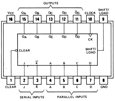
74195 IC 4-Bit Parallel-Access Shift Register
The IC 74195 is a 4-bit shift register that supports both serial input (SIPO) and parallel input (PIPO) operations. It can load 4-bit data in parallel or shift data serially, depending on control signals.
It has an asynchronous clear (CLR) input that immediately resets all outputs to LOW, independent of the clock. The parallel load (LOAD) input allows presetting a specific 4-bit value into the register. When LOAD is inactive, data is shifted serially from the serial input (SER) on each clock pulse.
The outputs (Q0–Q3) represent the register’s stored bits and can drive parallel circuits. The design ensures TTL compatibility and high-speed operation, making it suitable for data storage, transfer, and timing applications.
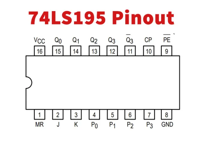
Pin Configuration (DIP-16)
| Pin | Name | Description |
|---|---|---|
| 1 | SER | Serial Data Input |
| 2 | CP | Clock Input |
| 3 | MR | Asynchronous Master Reset (LOW) |
| 4 | D0 | Parallel Data Input Bit 0 |
| 5 | D1 | Parallel Data Input Bit 1 |
| 6 | D2 | Parallel Data Input Bit 2 |
| 7 | D3 | Parallel Data Input Bit 3 (MSB) |
| 8 | GND | Ground |
| 9 | Q0 | Output Bit 0 |
| 10 | Q1 | Output Bit 1 |
| 11 | Q2 | Output Bit 2 |
| 12 | Q3 | Output Bit 3 (MSB) |
| 13 | PL | Parallel Load (active LOW) |
| 14 | ? | (Potential additional control pin – data varies by version) |
| 15 | ? | (Varies – may be enable or cascade) |
| 16 | VCC | +5V Power Supply |
(Exact pin labels may slightly differ across manufacturers; some versions label SER as DS, MR as CLR, and PL as LOAD.)
Key Features
4-bit serial-in/parallel-out register
Supports parallel loading of 4 bits
Asynchronous clear for immediate reset
TTL-compatible inputs and outputs
High-speed shifting capability
DIP-16 package
Applications
Expand microcontroller output lines.
Drive LED or numeric displays.
Convert serial data to parallel for storage.
Implement data buffering circuits.
Use in timing and delay line applications.
Design shift registers for cascading storage.
Build small memory registers.
Perform parallel-to-serial data conversions.
Teach register operations in labs.
Generate controlled bit sequences.
Specifications Table
| Parameter | Value |
|---|---|
| Logic Family | TTL |
| Function | Parallel-Access Shift Register |
| Number of Bits | 4 |
| Inputs | SER, CP, CLR, LOAD, D0–D3 |
| Outputs | Q0–Q3 |
| Input HIGH Voltage | ≥ 2.0V |
| Input LOW Voltage | ≤ 0.8V |
| Output HIGH Voltage | ≥ 2.4V |
| Output LOW Voltage | ≤ 0.4V ‘ |
| Propagation Delay | ~25 ns |
| Max Clock Frequency | ~25 MHz |
| Supply Voltage (Vcc) | 4.75V to 5.25V |
| Operating Temp | 0°C to 70°C |
| Package Type | DIP-16 / SOIC-16 |
| Number of Pins | 16 |