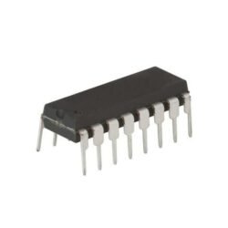

74164 IC 8-Bit Serial-In Parallel-Out Shift Register
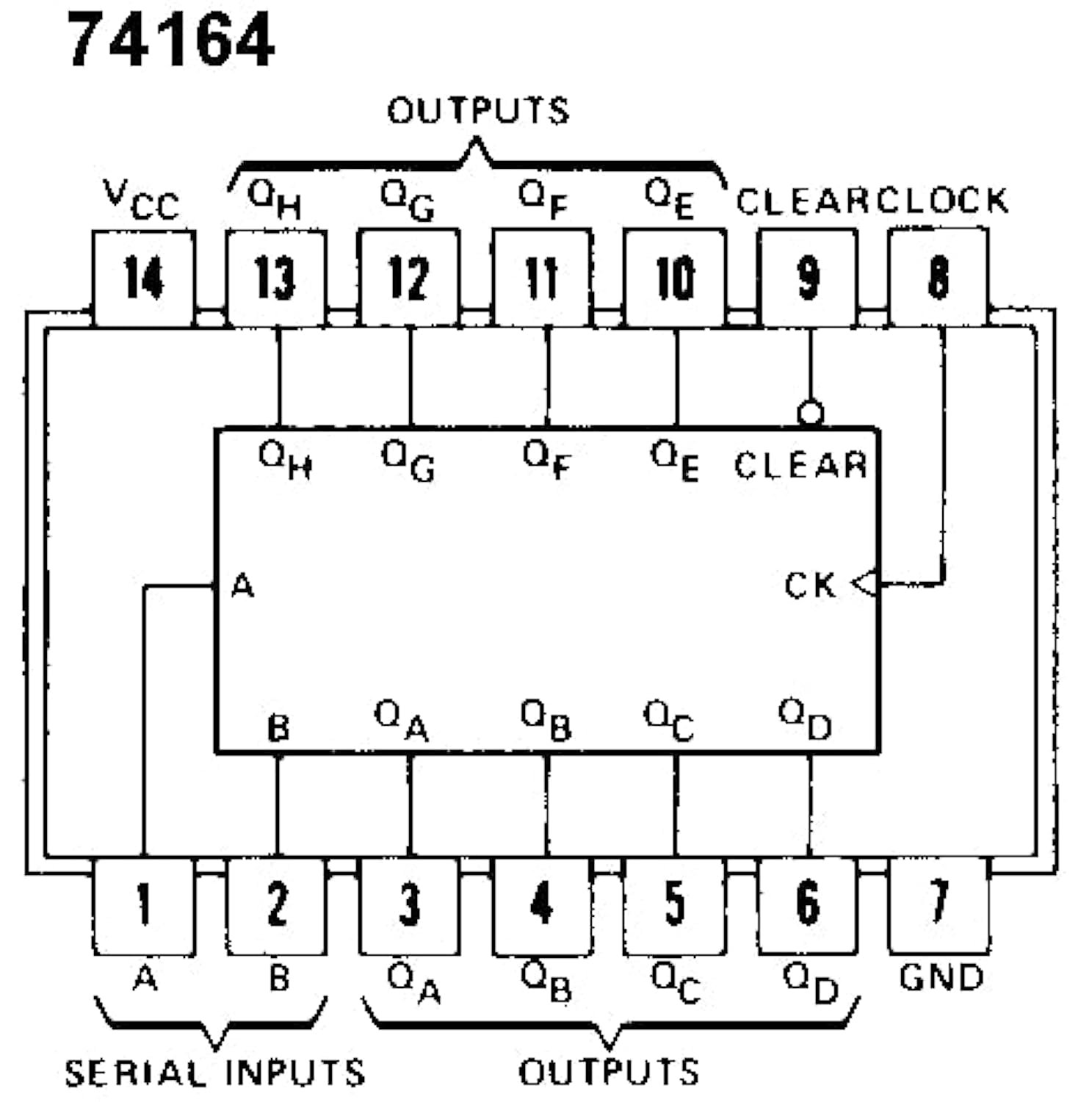
The IC 74164 is an 8-bit serial-in parallel-out (SIPO) shift register. It accepts serial data at its two inputs (A and B), which are logically ANDed, and shifts it into the register on each clock pulse. The data moves from the first flip-flop to the last, and the outputs (Q0–Q7) provide parallel access to each stored bit.
It features an asynchronous clear (CLR) that resets all outputs to LOW immediately, regardless of the clock. The 74164 is useful for data storage, serial-to-parallel conversion, and output line expansion.
Its TTL logic ensures compatibility with standard digital circuits, and its high-speed design makes it suitable for applications like LED driving, display control, and data buffering.
Pin Configuration (DIP-14)
| Pin | Name | Description |
|---|---|---|
| 1 | A | Serial Data Input A |
| 2 | B | Serial Data Input B |
| 3 | CLR | Asynchronous Clear (active LOW) |
| 4 | CLK | Clock Input |
| 5 | Q0 | Output Bit 0 (first stage) |
| 6 | Q1 | Output Bit 1 |
| 7 | Q2 | Output Bit 2 |
| 8 | GND | Ground |
| 9 | Q3 | Output Bit 3 |
| 10 | Q4 | Output Bit 4 |
| 11 | Q5 | Output Bit 5 |
| 12 | Q6 | Output Bit 6 |
| 13 | Q7 | Output Bit 7 (last stage) |
| 14 | VCC | +5V Power Supply |
Key Features
8-bit serial-in parallel-out operation
Two serial inputs (A and B) with internal AND gate
Asynchronous clear for immediate reset
TTL-compatible logic levels
High-speed shifting capability
Standard DIP-14 or SOIC-14 package
Applications
Expand microcontroller output lines.
Drive LED arrays or segment displays.
Convert serial data streams to parallel form.
Build simple data storage registers.
Create cascading registers for larger shifts.
Manage timing sequences in control circuits.
Buffer data between serial and parallel devices.
Use in keyboard encoding circuits.
Design digital delay lines.
Teach shift register behavior in labs.
Specifications Table
| Parameter | Value |
|---|---|
| Logic Family | TTL |
| Function | 8-bit SIPO Register |
| Number of Bits | 8 |
| Inputs | A, B, Clock, CLR |
| Outputs | Q0–Q7 |
| Input HIGH Voltage | ≥ 2.0V |
| Input LOW Voltage | ≤ 0.8V |
| Output HIGH Voltage | ≥ 2.4V |
| Output LOW Voltage | ≤ 0.4V ‘ |
| Propagation Delay | ~25 ns |
| Max Clock Frequency | ~25 MHz |
| Supply Voltage | 4.75V to 5.25V |
| Operating Temp | 0°C to 70°C |
| Package Type | DIP-14 / SOIC-14 |
| Number of Pins | 14 |