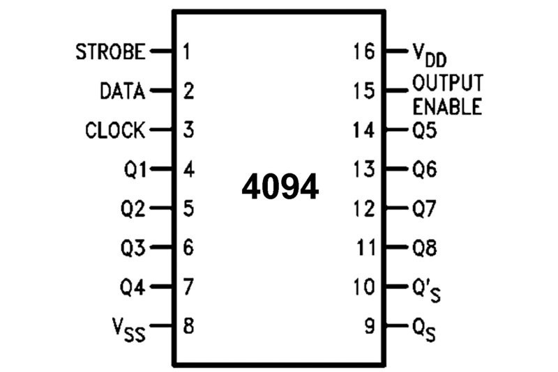


4094 IC 8-Stage Serial Shift Register
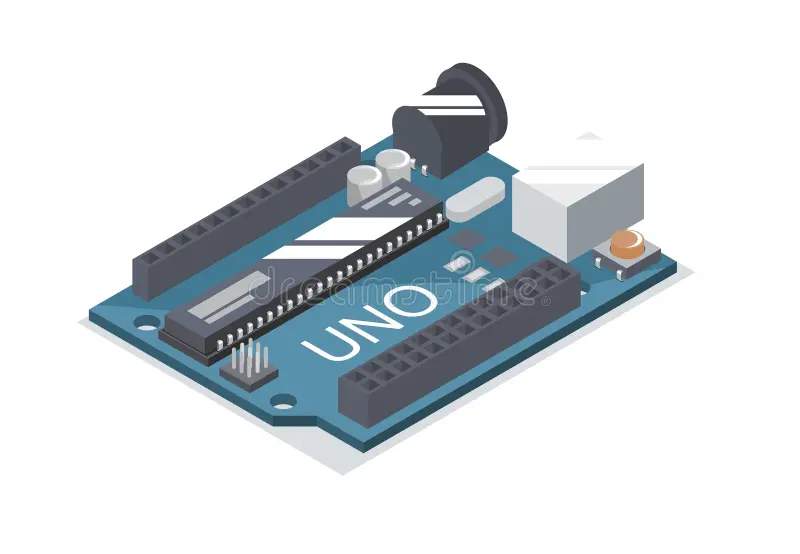
The CD4094BE is a highly efficient 8-stage serial-in/parallel-out shift register with output latches, designed for expanding output capabilities in digital systems. Engineers use this IC to convert serial data into parallel output across eight Q outputs. The device features both serial and parallel data output options, enabling seamless integration in microcontroller-based systems requiring additional I/O lines.
Each stage includes a D-type master-slave flip-flop with its own output latch, which allows the data to be latched independently from the shifting operation. With Schmitt Trigger inputs, the IC provides high noise immunity, ensuring reliable operation in electrically noisy environments. It operates across a wide voltage range of 3V to 15V, and its low power consumption makes it ideal for battery-powered and embedded systems.
Key Features
8-bit shift register with parallel output latches
Serial data input (D) and serial output (Q_S)
Independent latch enable and clock inputs
Cascade capability via Q_S output
Buffered parallel outputs (Q1 to Q8)
Wide supply voltage range: 3V to 15V
High noise immunity with Schmitt Trigger inputs
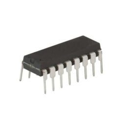
DIP-16 package for easy breadboarding
Product Specifications
| Specification | Value |
|---|---|
| Professional Name | CD4094BE |
| Logic Type | Serial-In Parallel-Out Shift Register |
| Logic Family | CMOS |
| Number of Bits | 8 ‘ |
| Data Inputs | Serial-In (D), Clock, Latch Enable |
| Outputs | 8 Parallel (Q1–Q8) + Serial Out (Q_S) |
| Output Type | Buffered CMOS |
| Supply Voltage Range | 3V to 15V |
| Max Clock Frequency | 8 MHz at 10V |
| Package Type | DIP-16 |
| Operating Temperature | -55°C to +125°C |
Pin Configuration (DIP-16)
| Pin No. | Name | Description |
|---|---|---|
| 1 | Q5 | Parallel Output 5 |
| 2 | Q6 | Parallel Output 6 |
| 3 | Q7 | Parallel Output 7 |
| 4 | Q8 | Parallel Output 8 |
| 5 | Q_S | Serial Output |
| 6 | Clock | Shift Register Clock Input |
| 7 | Strobe | Latch Enable Input |
| 8 | GND | Ground |
| 9 | D | Serial Data Input |
| 10 | MR | Master Reset (Active Low) |
| 11 | Q1 | Parallel Output 1 |
| 12 | Q2 | Parallel Output 2 |
| 13 | Q3 | Parallel Output 3 |
| 14 | Q4 | Parallel Output 4 |
| 15 | Enable | Output Enable (Active Low) |
| 16 | VDD | Positive Supply Voltage |
Applications
Expanding digital I/O lines in microcontroller systems
LED matrix control and digital display drivers
Data acquisition and storage buffers
Industrial automation and control panels
Signal processing and timing control circuits