


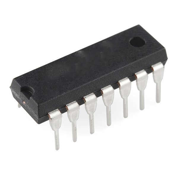
4093 IC Quad 2-Input NAND Schmitt Trigger
The CD4093BE is a versatile CMOS logic IC that integrates four 2-input NAND gates with Schmitt Trigger inputs. It enhances noise immunity and signal integrity in digital systems by combining the NAND logic function with hysteresis on each input, thanks to the built-in Schmitt Trigger action. This feature allows the IC to clean up noisy or slow-changing input signals, making it ideal for waveform shaping, signal conditioning, and debounce circuits.
This quad NAND gate operates efficiently across a wide supply voltage range of 3V to 15V, making it suitable for both TTL and CMOS environments. Each gate responds with rapid switching while maintaining low power consumption. Its robust construction supports a wide temperature range, making it a reliable solution for industrial, educational, and prototyping applications.
Key Features
Four independent 2-input NAND gates
Schmitt Trigger inputs on all gates
High noise immunity
Wide supply voltage range: 3V to 15V
Low static power consumption
TTL-compatible input and output voltage levels
DIP-14 through-hole package
Excellent for waveform shaping and debounce applications
Product Specifications
| Specification | Value |
|---|---|
| Professional Name | CD4093BE |
| Logic Type | Quad NAND Gate with Schmitt Trigger |
| Logic Family | CMOS |
| Number of Gates | 4 |
| Inputs per Gate | 2 ‘ |
| Schmitt Trigger | Yes (on all inputs) |
| Supply Voltage Range | 3V to 15V |
| Input Voltage Range | 0V to VDD |
| Output Type | Buffered CMOS |
| Package Type | DIP-14 |
| Operating Temperature | -55°C to +125°C |
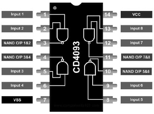
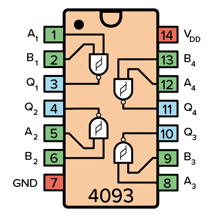
Pin Configuration (DIP-14)
| Pin No. | Name | Description |
|---|---|---|
| 1 | A1 | Input A of Gate 1 |
| 2 | B1 | Input B of Gate 1 |
| 3 | Y1 | Output of Gate 1 (A1 NAND B1) |
| 4 | A2 | Input A of Gate 2 |
| 5 | B2 | Input B of Gate 2 |
| 6 | Y2 | Output of Gate 2 (A2 NAND B2) |
| 7 | GND | Ground |
| 8 | Y3 | Output of Gate 3 (A3 NAND B3) |
| 9 | A3 | Input A of Gate 3 |
| 10 | B3 | Input B of Gate 3 |
| 11 | Y4 | Output of Gate 4 (A4 NAND B4) |
| 12 | A4 | Input A of Gate 4 |
| 13 | B4 | Input B of Gate 4 |
| 14 | VDD | Positive Supply Voltage |
Applications
Signal debouncing for switches and buttons
Waveform shaping and signal conditioning
Digital pulse generation
Square wave oscillators
Logic gating in noisy environments
Educational and lab logic circuit demonstrations