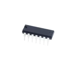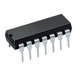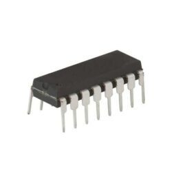
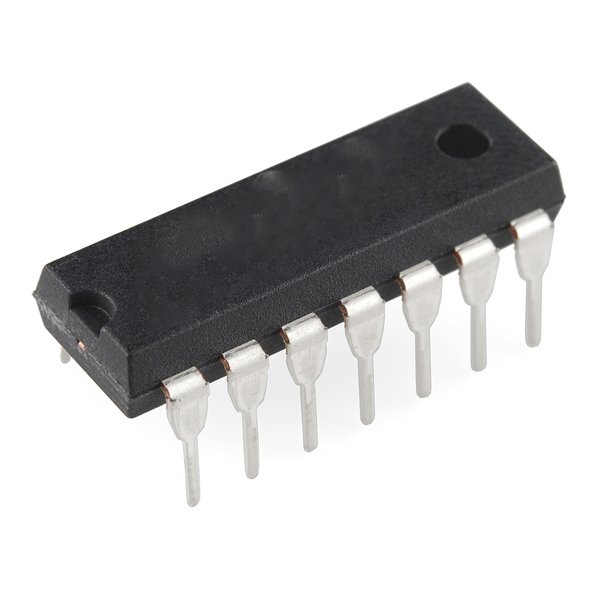

4047 IC Monostable/Astable Multivibrator CMOS
The CD4047BE is a flexible CMOS multivibrator IC that delivers monostable and astable operation modes with precise timing control. Designed using low-power CMOS technology, it offers reliable performance in timer, oscillator, and pulse generator applications.
In astable mode, the IC functions as a free-running oscillator with user-defined frequency and duty cycle, determined by external resistor and capacitor values. In monostable mode, it produces a single pulse of specified duration triggered by a rising or falling edge. This versatility allows designers to use a single chip for a variety of timing tasks.
Key Features
Supports both monostable and astable modes
Wide supply voltage range: 3V to 15V
Low power consumption with CMOS technology
Buffered complementary outputs (Q and Q̅)
High noise immunity
Precise frequency and pulse width control
Compatible with TTL and CMOS logic
14-pin DIP package
Pin Configuration (14-Pin DIP Package)
| Pin No | Symbol | Description |
|---|---|---|
| 1 | A̅ | Negative edge trigger input (monostable) |
| 2 | B | Positive edge trigger input (monostable) |
| 3 | CEXT | External timing capacitor |
| 4 | REXT | External timing resistor |
| 5 | CONT | Control voltage (optional) |
| 6 | Q | Normal output |
| 7 | Q̅ | Complementary output |
| 8 | GND | Ground ‘ |
| 9 | NC | Not connected |
| 10 | ASTABLE | Astable mode enable |
| 11 | RESET | Reset input |
| 12 | MONO | Monostable mode enable |
| 13 | NC | Not connected |
| 14 | VDD | Positive power supply |
Applications
Monostable and astable timers
Frequency generators
Pulse width modulation
Clock pulse generation
Oscillators for tone generation
Time delay circuits
LED and lamp flashers
Digital timing in embedded systems
Product Specifications
| Specification | Value |
|---|---|
| IC Name | CD4047BE |
| Function | Monostable / Astable Multivibrator |
| Technology | CMOS |
| Operating Voltage Range | 3V to 15V |
| Output Current (per pin) | ±10 mA (maximum) |
| Input Logic Level High | ≥ 70% of VDD |
| Input Logic Level Low | ≤ 30% of VDD |
| Power Consumption | Low (typical CMOS levels) |
| Package Type | DIP-14 |
| Temperature Range | -55°C to +125°C |
| Frequency Stability | High (depends on R and C values) |
| Propagation Delay | ~100 ns (varies with VDD) |
| Output Type | Buffered Q and Q̅ |
| Reset Pin | Active High |