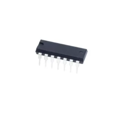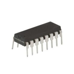

40104 IC 4-Bit Pipo Universal Shift Register
data transfer with precision and control. Engineers often use this IC in digital circuits requiring flexible data routing, temporary storage, or serial-to-parallel and parallel-to-serial data conversions. BOperating over a wide voltage range of 3V to 15V, the CD40104 is ideal for embedded systems, control logic, and memory interfacing. Its high noise immunity and low static power consumption make it reliable even in harsh electrical environments.
This IC supports parallel loading, left or right shifting, and data holding, all controlled by dedicated logic inputs. Each mode of operation is determined by two mode-select inputs, making it highly adaptable to various logic applications. The design includes internal D-type flip-flops, ensuring synchronized clocked operations.
Key Features
4-bit universal shift register
Bidirectional shifting (left and right)
Parallel data loading capability
Mode control inputs for flexible operations
Separate clock input for synchronization
Wide supply voltage: 3V to 15V
High noise immunity
DIP-16 package
Product Specifications
| Specification | Value |
|---|---|
| Professional Name | CD40104BE |
| Logic Type | Universal Shift Register |
| Bit Width | 4-bit |
| Shift Direction | Left or Right |
| Data Handling | Serial and Parallel |
| Control Inputs | Mode Select (S1, S0), Clock, Reset |
| Output Type | CMOS Buffered |
| Supply Voltage Range | 3V to 15V ‘ |
| Max Clock Frequency | ~8 MHz @ 10V |
| Package Type | DIP-16 |
| Operating Temperature | -55°C to +125°C |
Pin Configuration (DIP-16)
| Pin No. | Name | Description |
|---|---|---|
| 1 | Q1 | Parallel Output Bit 1 |
| 2 | Q2 | Parallel Output Bit 2 |
| 3 | Q3 | Parallel Output Bit 3 |
| 4 | Q4 | Parallel Output Bit 4 |
| 5 | MR | Master Reset (active high) |
| 6 | S0 | Mode Control Input 0 |
| 7 | S1 | Mode Control Input 1 |
| 8 | GND | Ground |
| 9 | Clock | Clock Input |
| 10 | SI | Serial Data Input |
| 11 | PL | Parallel Load Control Input |
| 12 | A | Parallel Data Input Bit A (MSB) |
| 13 | B | Parallel Data Input Bit B |
| 14 | C | Parallel Data Input Bit C |
| 15 | D | Parallel Data Input Bit D (LSB) |
| 16 | VDD | Positive Supply Voltage |
Applications
Data storage and transfer systems
Serial-to-parallel / parallel-to-serial converters
Digital data buses and temporary buffers
Microcontroller I/O expansion
Signal manipulation in control logic