
4052 IC dual 4-channel analog demultiplexer
The CD4052BE is a dual 4-channel analog multiplexer/demultiplexer IC designed for high-performance signal routing applications. This versatile chip handles both analog and digital signals, enabling users to connect one of four inputs/outputs to a common terminal for each channel. With independent control of each multiplexer via select lines, the IC provides flexibility in data acquisition systems, analog switching, and microcontroller interfacing.
The IC supports rail-to-rail analog signal handling, making it suitable for applications that require low signal distortion and high accuracy. Its CMOS construction ensures low power consumption, high noise immunity, and a wide operating voltage range from 3V to 15V. Engineers and hobbyists alike use this component in sensor multiplexing, instrumentation, communication circuits, and microcontroller-based systems where signal control and channel switching are critical.
Key Features
Dual 4-channel analog multiplexer/demultiplexer
Independent control for each 4:1 MUX
Bidirectional signal transmission (analog and digital)
Wide supply voltage range: 3V to 15V
Low power CMOS design
Rail-to-rail signal range support
Low ON resistance and high OFF isolation
High noise immunity and fast switching
TTL/CMOS compatible inputs
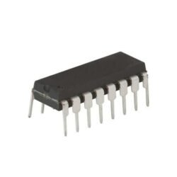
DIP-16 package for easy prototyping
Product Specifications
| Specification | Value |
|---|---|
| Professional Name | CD4052BE |
| Function Type | Dual 4-Channel Analog Multiplexer |
| Technology | CMOS |
| Number of Channels | 2 (4:1 multiplexers) |
| Signal Type | Analog and Digital |
| Supply Voltage (VDD) | 3V to 15V |
| Control Inputs | A, B, INH |
| Common Outputs | Y (X and Y multiplexers) |
| Max Channel Resistance | ~125 Ohms @ VDD = 5V |
| Leakage Current | < 0.1 μA ‘ |
| Max Propagation Delay | ~200 ns |
| Operating Temp. Range | -55°C to +125°C |
| Package Type | DIP-16 |
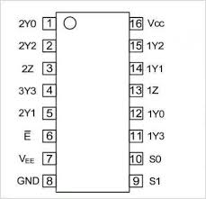
Pin Configuration (DIP-16)
| Pin No. | Name | Description |
|---|---|---|
| 1 | Y0 | Channel 0 of multiplexer Y |
| 2 | Y2 | Channel 2 of multiplexer Y |
| 3 | Y1 | Channel 1 of multiplexer Y |
| 4 | Y3 | Channel 3 of multiplexer Y |
| 5 | COM Y | Common output/input for multiplexer Y |
| 6 | COM X | Common output/input for multiplexer X |
| 7 | X3 | Channel 3 of multiplexer X |
| 8 | GND | Ground |
| 9 | X0 | Channel 0 of multiplexer X |
| 10 | X2 | Channel 2 of multiplexer X |
| 11 | X1 | Channel 1 of multiplexer X |
| 12 | X3 | Channel 3 of multiplexer X |
| 13 | INH | Inhibit (active high disables switches) |
| 14 | A | Select line A (LSB) |
| 15 | B | Select line B (MSB) |
| 16 | VDD | Positive Supply Voltage |
Applications
Sensor input selection systems
Audio signal switching
Analog signal routing in DAQ systems
Control systems with multiple I/O
Digital communication circuits
Robotics and automation interfaces